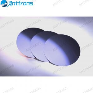
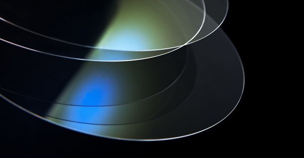
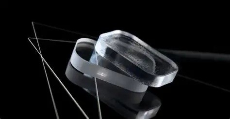
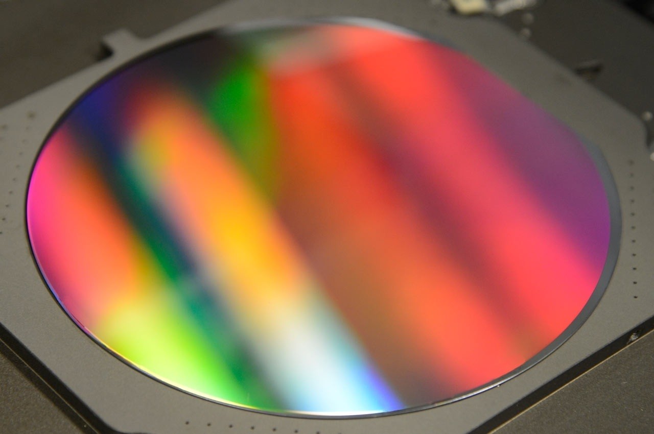
Wafer-Level Optic Solutions
- Product Item : AT-61150
- Category: Optical semiconductor materials
- Product description:
Wafer-Level Optic Solutions
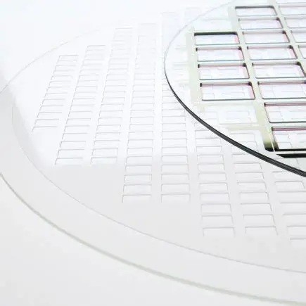
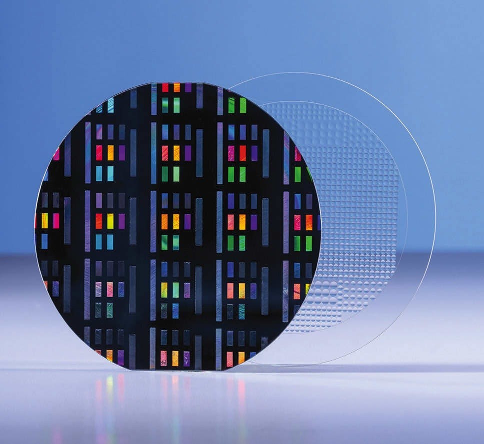
Applications
Micro-optics and substrates
Refractive and difractive optical elements (ROEs & DOEs)
3D sensors, optics, spacers, heat sinks, and camera optics
Beam shaping elements
Homogenizers and optical sensors
RF components
Nanoimprint lithography substrates
Hard disk masters and molds
Blazed-wavelength and sub-wavelength difraction gratings
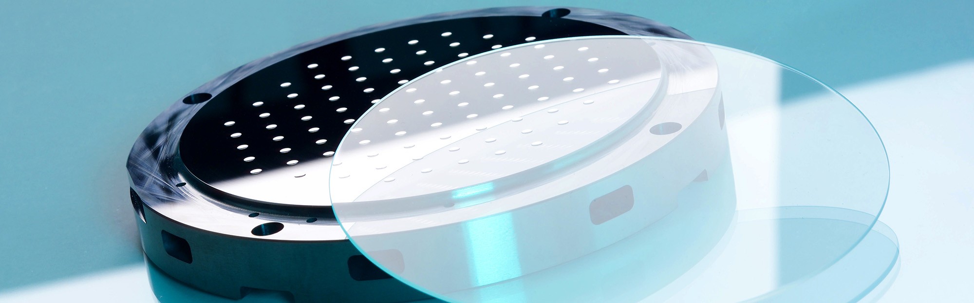
Beneits of Wafer-Level Optic Solutions
Various melting and forming methods enable signiicant volume supply of high-precision wafers with lowest
thickness variation: part to part and batch to batch
Compatible with wafer-level optic and semicon manu- facturing processes anlegacy
equipment and tools
Supporting capabilities include ceramics, automated laser glass-cutting,
photostructuring, bonding, dicing, and coatings
Best-in-class metrology minimizes reliability risks and enables ine resolution data
across the full wafer
Fracture mechanics glass strength experts available to train and consult on many
applications
Material Properties and Attributes
Diameters: 100/150/200/300 mm
Diameter tolerance*: +/- 0.200 mm
Thickness range: 0.10-5.0 mm
Thickness tolerance*: +/- 0.020 mm
Available upon request: Various sizes/shapes/features, semi notch/lat speciications, laser serialization, laser processing, structuring, holes, bonding, coatings
Large volume capacity: up to 60k WPM
Typical lead-time: 2-12 weeks
Polish scratch/dig: 20/10 to 80/50 per military spec
World-class MSP metrology
*Other tighter tolerances available upon request
Multiple Compositions* for Diverse Applications
|
Glass/CTE |
Abbe Value vD |
RefractiveIndex nD |
|
SG 0.5 |
67.8 |
1.459 |
|
SG 5.1 |
65.0 |
1.487 |
|
SG 7.1 |
60.7 |
1.492 |
|
SG 7.8 |
61.7 |
1.496 |
|
SG 3.4 |
62.7 |
1.510 |
|
SG 3.6 |
62.7 |
1.510 |
|
SG 8.2 |
64.2 |
1.517 |
|
SG 9.3 |
58.9 |
1.523 |
|
SG 9.5 |
57.1 |
1.523 |
|
SG 3.8 |
61.9 |
1.523 |
|
SG 3.7 |
61.1 |
1.527 |
|
SG 9.0 |
55.6 |
1.530 |
|
SG 10.0 |
41.6 |
1.601 |
*Active glasses shown here; Others available upon request
Typical Properties and Attributes
|
TTV |
≤ 1 µm to ≤ 5µm |
|
Bow |
≤ 5µm to ≤ 30µm |
|
Warp |
+/- 20µm to ± 40µm |
|
Surface roughness (Ra) |
≤ 10Å |
|
SORI |
≤ 0.5µm to ≤ 1.5µm |