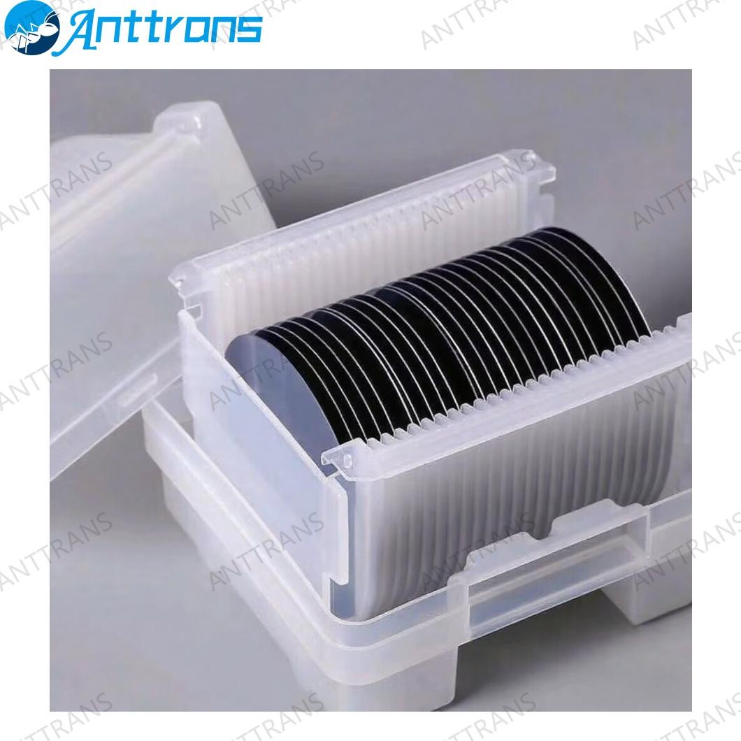
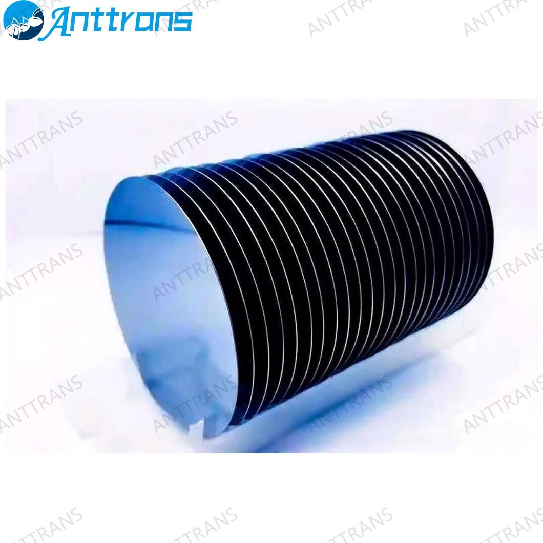
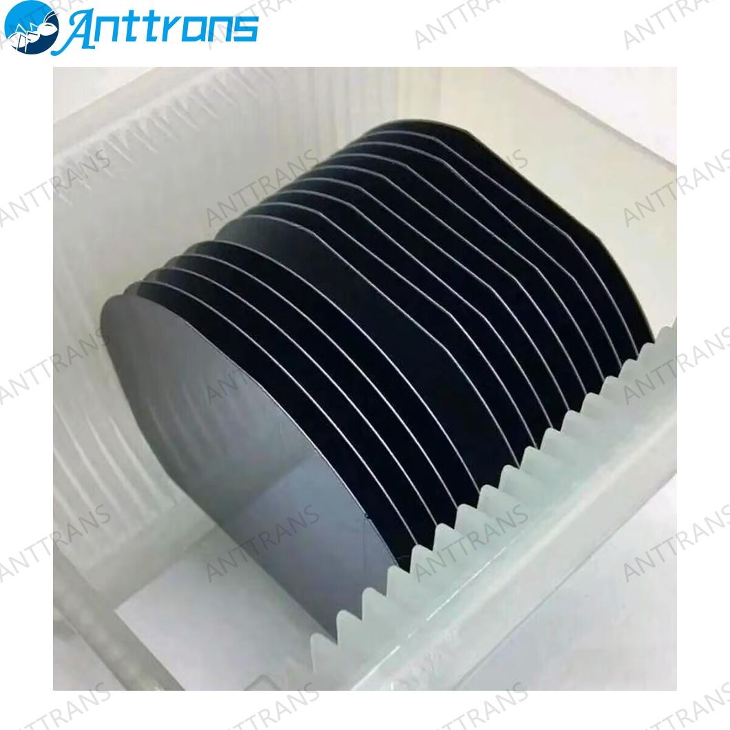
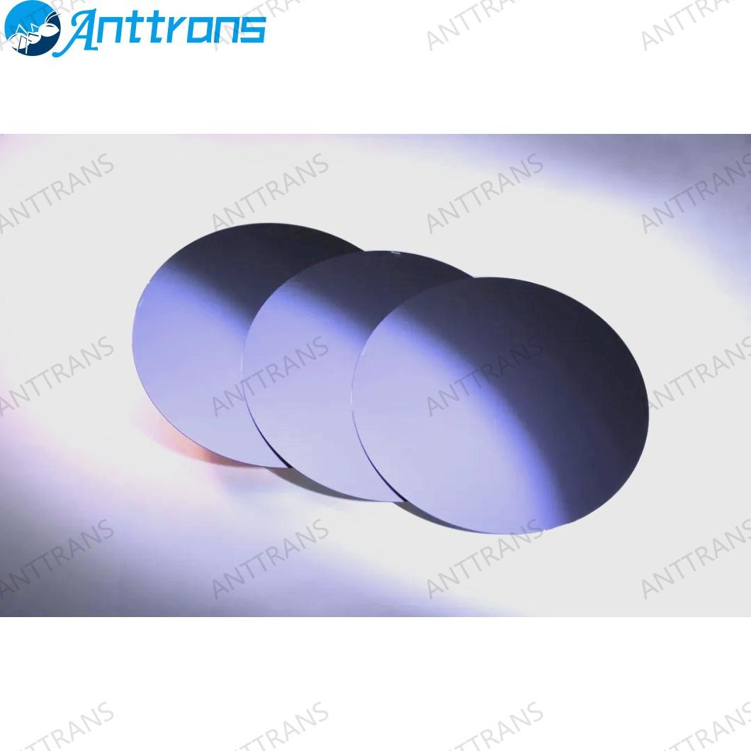
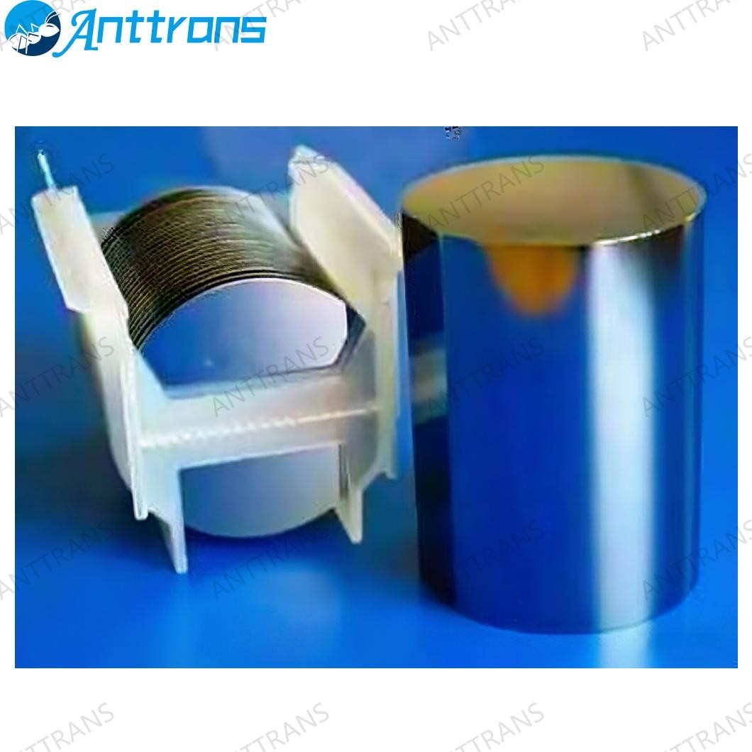

6-Inch Silicon Wafer
- Product Item : AT-61057
- Category: Optical Fiber, Quartz & Semiconductor Consumables
- Product description:
Silicon wafers are thin slices made primarily of high-purity silicon and serve as the core substrate for semiconductor devices and solar cells.
I. Basic Characteristics
Material Source: Silicon constitutes 25.8% of the Earth's crust, making it abundant and cost-effective to mine, an ideal choice for large-scale applications such as solar cells.
Purity Requirements: Semiconductor-grade silicon must achieve an ultra-high purity of 11 nines (99.999999999%), while photovoltaic-grade silicon typically ranges from 6N to 9N.
II . Types and Applications
Monocrystalline Silicon Wafers
Manufactured by slicing monocrystalline silicon ingots, these wafers have a complete crystal lattice structure, exhibiting excellent conductivity and photoelectric conversion efficiency.
Used in semiconductor chips (such as CPUs) and high-performance solar cells, capable of integrating over 40 million transistors.
Available in circular (for semiconductor use) or rounded square (for photovoltaic use) shapes.
Polycrystalline Silicon Wafers
Composed of randomly arranged silicon grains, these wafers are cost-effective but offer lower efficiency, primarily used in low-end solar cells.
Quasi-Square Monocrystalline Silicon Wafers
Produced through the ingot casting method, these square wafers combine the performance of monocrystalline silicon with the cost advantages of polycrystalline silicon. They increase silicon material utilization from 50% to 65%, significantly reducing the cost of solar cells.
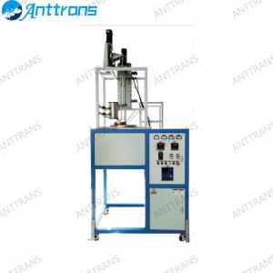
III. Preparation Process
Semiconductor silicon wafers undergo a complex process:
Monocrystalline Growth: Silicon ingots are produced using the Czochralski (CZ) method or the Float Zone (FZ) method.
Slicing and Grinding: The ingots are sliced into 500-700 micron thick wafers using multi-wire cutting, followed by chamfering to prevent edge stress.
Surface Treatment: Chemical etching (using a mixture of hydrofluoric acid and nitric acid) removes the damaged layer, followed by chemical mechanical polishing (CMP) to achieve sub-micron level flatness.
Inspection: Geometric dimensions, surface finish, and electrical performance are inspected to ensure compliance with chip manufacturing requirements.
IV. Application Areas
Semiconductors: Logic chips, memory chips, etc. 12-inch wafers dominate the market (with a global market share of 69.15%), directly influencing chip performance and yield.
Photovoltaics: Core material for solar cell wafers, with monocrystalline silicon wafers achieving conversion efficiencies of 17%-25%, superior to polycrystalline silicon wafers (below 15%).
Others: Aerospace, industrial equipment, and agricultural sensors, etc.
V. Core Advantages
Physical Properties: Silicon's semiconductor properties are stable, suitable for high-temperature and high-frequency operating environments.
Economy: Abundant resources and recyclability significantly reduce large-scale production costs.