


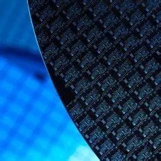
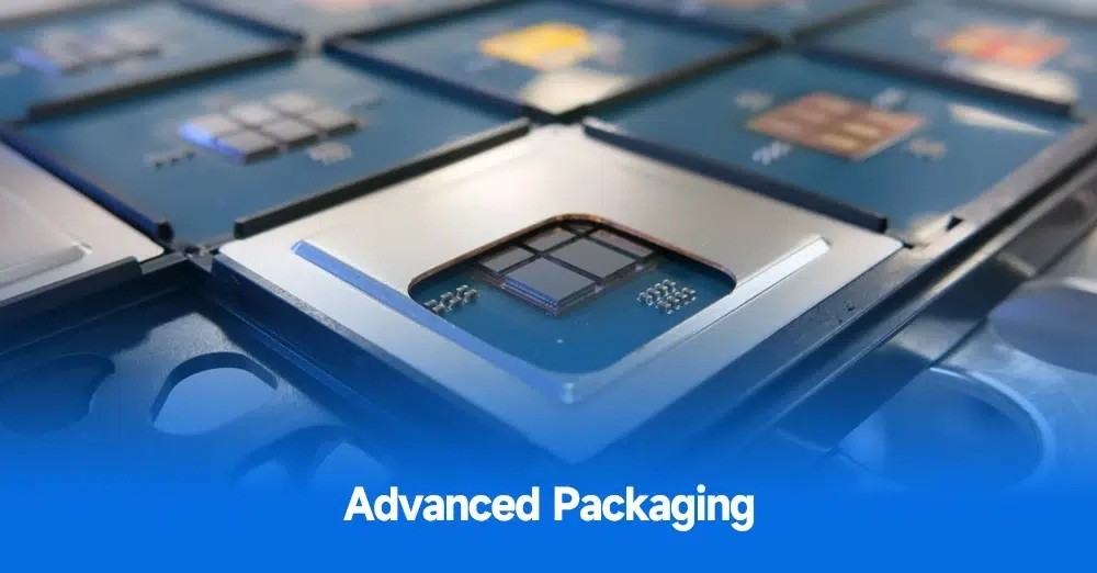
Advanced Packaging Carriers
- Product Item : AT-61146
- Category: Optical Cover Glass Materials
- Product description:Glass carriers for temporary bonding in advanced semiconductor packaging processes such as fan-out level processing
Advanced Packaging Carriers
Applications
Glass carriers for temporary bonding in advanced semiconductor packaging processes such as fan-out level processing
Benefits
Specially developed to reduce customers' challenge of in-process warp by up to 40%
Available in fine granularities across a range of CTEs up to 12.6ppm/⁰C
High stiffness to help overcome CTE mismatch challenge
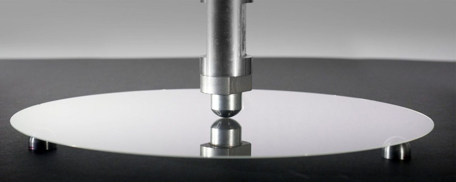
Ultra low TTV and warp
Excellent chemical durability conducive to semiconductor process environments
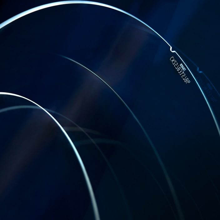
Optically transparent enabling UV or IR based debond processes and laser mark serialization
|
Property |
SG-HS |
SG-HC |
|
CTE (0-300⁰C, x10-6/⁰C) |
4.9-7.9 |
9.6-12.6 |
|
Density (g/cm3) |
2.56-2.57 |
2.50-2.51 |
|
Young’s Modulus (GPa) |
80-87 |
75-78 |
|
Shear Modulus (GPa) |
32-34 |
30-32 |
|
Vicker's Hardness (kgf/mm2)200gm load |
635-670 |
635-670 |
|
Annealing Point (⁰C) |
600-680 |
440-510 |
|
Strain Point (⁰C) |
560-640 |
400-470 |
|
Refractive Index (589.3nm) |
1.54-1.55 |
1.52-1.53 |
|
CTE Granularity (x10-6/⁰C) |
0.2 |
0.4 |
|
Poisson’s Ratio |
0.26-0.27 |
0.23-0.24 |
|
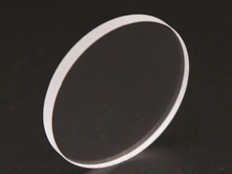
Diameter (mm) |
100-300 |
|
Thickness |
0.4 to 2.0 |
|
Edge Beveling |
Radius (R) Type and Chamfer (C) |
|
Surface Roughness |
< 1.0nm |
|
Features |
Semi-standard notch/flat or custom |
|
Surface ID Marking |
Semi-standard or custom |