

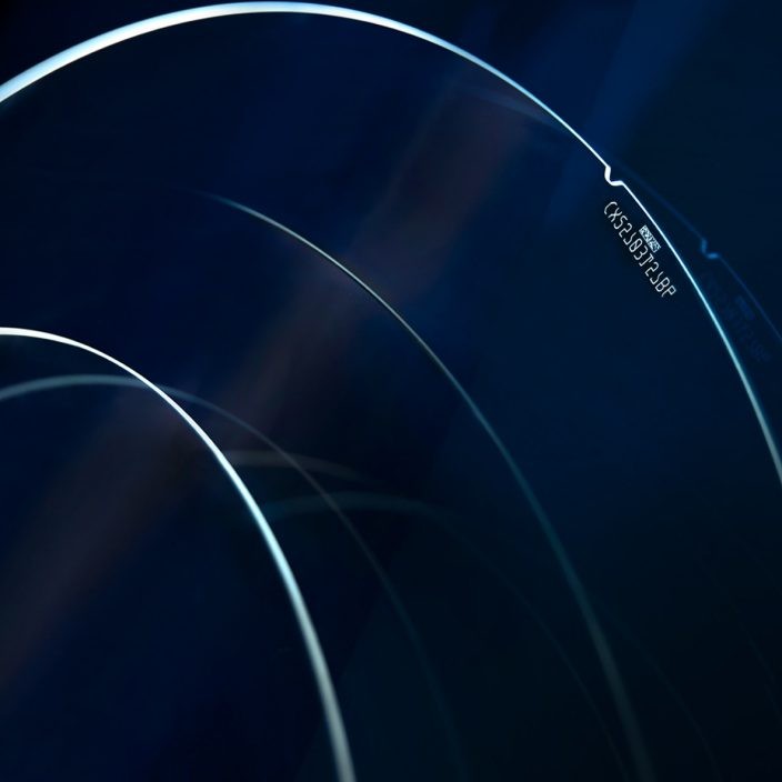
Ultra-Low TTV Glass Wafers
- Product Item : AT-61147
- Category: Optical semiconductor materials
- Product description:Our Ultra-Low TTV Glass Wafers have superior surface quality, flexible thickness, and can be available in a wide range of CTEs to meet customers’ most challenging requirements – from research & devel
Ultra-Low TTV Glass Wafers
Our Ultra-Low TTV Glass Wafers have superior surface quality, flexible
thickness, and can be available in a wide range of CTEs to meet customers’ most challenging requirements – from research & development phase to mass production.
Applications
This glass wafer has one of the lowest TTV currently available and enables advanced semiconductor manufacturing as well as RF applications for 5G connectivity and hybrid bonding.
Enables ultra-thinning of device wafer (final thickness<10μm)
Allows more TTV tolerance for the adhesive layer to achieve same total stack TTV in semiconductor packaging
Supports existing temporary bonding infrastructure to enable thinner device wafers
Improves yield of Z-height sensitive processes
Benefits
TTV 0.2μm is available in sizes up to 200mm (3mm edge exclusion)
TTV 0.4μm is available in sizes up to 300mm (2mm edge exclusion)
This product is available now in a range of thicknesses for a variety of glass compositions.
Available in across a range of CTEs from 3.4 to 12.6 ppm/⁰C
High stiffness to help overcome CTE mismatch challenge
Optically transparent enabling UV or IR based debond processes and laser mark serialization
Options and Features
|
Diameter (mm) |
100-300 |
|
Thickness (mm) |
0.5 to 1.0 |
|
Edge Beveling |
Radius (R) Type and Chamfer (C) |
|
Surface Roughness (nm) |
< 1.0 |
|
Features |
Semi-standard notch/flat or custom |
|
Surface ID Marking |
Semi-standard or custom |