


Standard Glass Carriers
- Product Item : AT-61145
- Category: Optical Cover Glass Materials
- Product description:Glass carriers for temporary bonding in advanced semi-conductor packaging processes such as Silicon wafer thinning and fan-out level processing
Standard Glass Carriers
Applications
Glass carriers for temporary bonding in advanced semi-conductor packaging processes such as Silicon wafer thinning and fan-out level processing
Benefits
Tunable CTE and mechanical properties to meet various semiconductor process requirements
Scalable form factor in both wafer and panel formats Low TTV and warp
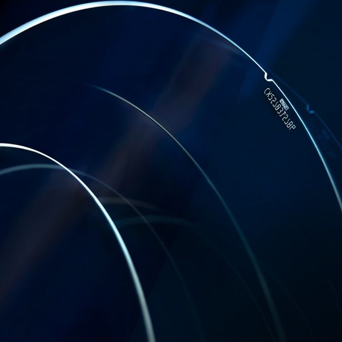
Optically transparent enabling UV or IR based debond processes and laser mark serialization
Excellent chemical durability conducive to semiconductor process environments
|
Property |
SG 3.4 |
SG 7.8 |
SG 9.0 |
|
CTE (0-300⁰C, x10-6/⁰C) |
3.4 |
7.8 |
9.0 |
|
Density (g/cm3) |
2.38 |
2.39 |
2.42 |
|
Young’s Modulus (GPa) |
73.6 |
69.3 |
65.8 |
|
Shear Modulus (GPa) |
30.1 |
28.5 |
26.0 |
|
Vicker's Hardness (kgf/mm2)200gm load |
640 |
534 |
489 |
|
Annealing Point (⁰C) |
722 |
628 |
646 |
|
Strain Point (⁰C) |
669 |
574 |
596 |
|
Refractive Index (589.3nm) |
1.51 |
1.50 |
1.49 |
|
CTE Offerings |
3.4 x10⁻⁶/ºC – 10x10-6/ºC |
|
Form Factors |
Wafers: 100mm – 450mm Panels: Up to 600mm x 600mm |
|
Thickness |
Wafers: 0.4mm – 1.1mm Panels: 0.7mm - 2.0mm |
|
Edge Beveling |
Radius (R) Type and Chamfer (C) |
|
Surface Roughness |
< 1.0nm |
|
Features |
Wafers: Semi-standard notch/flat Panels: Orientation corner profiles |
|
Surface ID Marking |
Semi-standard or custom |